The history of photovoltaics is, in part, a history of learning to control boundaries. In 1839, the French physicist Alexandre-Edmond Becquerel noticed that light could produce an electric current in an electrochemical cell. More than a century later, Bell Laboratories scientists Daryl Chapin, Calvin Fuller, and Gerald Pearson built the first practical silicon solar cell in 1954. Their device transformed a fragile physical effect into useful technology, but its central architecture remained familiar: light enters a semiconductor, creates electrons and holes, and an internal electric field separates them before they recombine.
Today, a new generation of researchers is revisiting that architecture with materials only a few atoms thick. These are two-dimensional, or 2D, crystals: sheets in which atoms are strongly bonded within a plane but interact relatively weakly between planes. Graphene, isolated in 2004 by Andre Geim and Konstantin Novoselov, made the idea famous. Other layered materials—molybdenum disulfide, tungsten diselenide, black phosphorus, and many related compounds—offer something graphene does not: a semiconductor band gap that can absorb and emit light.
The interface becomes the device
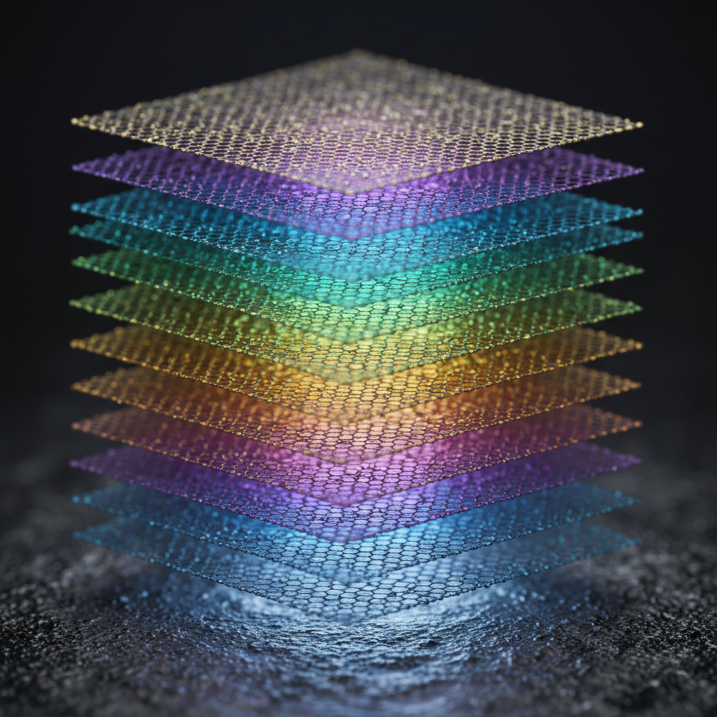
A single atomic sheet is remarkable, but the more consequential idea is to stack different sheets into a heterostructure. In conventional electronics, joining two semiconductors requires close control of crystal lattices and chemical processing. 2D crystals can be placed together even when their atomic patterns do not match perfectly, because their surfaces have no dangling bonds. The resulting interface is clean, thin, and unusually adjustable.
In 2013, researchers including Andres Geim, Kostya Novoselov, and colleagues demonstrated van der Waals heterostructures by combining graphene with hexagonal boron nitride and other atomically thin materials. The work established a kind of materials Lego: crystals could be assembled layer by layer, with properties determined not only by composition but also by order, spacing, twist angle, and electrostatic environment.
For photovoltaics, this flexibility addresses a fundamental tension. A solar absorber should capture a broad range of sunlight, yet the charges it creates must travel to contacts before they disappear. One semiconductor may absorb strongly while another transports charge efficiently. A third may form an energetic barrier that directs electrons and holes in opposite directions. Stacking them can separate these tasks.
Harvesting light at the limit
Atomically thin semiconductors interact strongly with light despite their small volume. In materials such as molybdenum disulfide and tungsten diselenide, electrons and holes can bind into excitons—quasiparticles resembling hydrogen atoms. At a junction between dissimilar 2D layers, band alignment can favor the migration of an electron into one sheet and the hole into another. This spatial separation can suppress recombination and create a measurable photovoltaic response.
The layers can also be rotated. When two similar crystals are stacked with a small angular mismatch, their lattices form a long-range moiré pattern. This superlattice can reshape electronic states and exciton motion, offering a route to tune absorption and charge separation without changing chemical composition. In principle, a solar cell could be designed as an optical and electronic landscape, with different regions engineered to perform different functions.
There is an important catch: atomically thin absorbers do not intercept much sunlight. A practical device therefore may require many layers, optical cavities, concentrators, or hybrid architectures combining 2D materials with thicker absorbers such as silicon or perovskites. The 2D component may serve as an absorber, a charge-selective contact, a passivation layer, or an interfacial catalyst rather than as the entire cell.
From elegant flakes to reliable technology
The distance between a striking laboratory measurement and a solar module is substantial. Researchers must control defects, contamination, wrinkles, and contact resistance across large areas. Some promising materials degrade in oxygen, moisture, or intense illumination. Transfer methods developed for tiny exfoliated flakes are difficult to scale, while chemical vapor deposition and other growth techniques can introduce grain boundaries and nonuniformity.
Efficiency is only one test. A photovoltaic technology must also survive heat, light, mechanical stress, and years of operation. It must use abundant or responsibly sourced elements, permit economical manufacturing, and fit within existing module processes. These constraints have redirected the field from the simple question—“Can a 2D material make electricity from light?”—to a more demanding one: “Which atomic interface improves the whole device?”
A solar future written at the boundary
The enduring importance of 2D heterostructures is therefore not that they promise a single miraculous absorber. Their deeper contribution is conceptual. They make the interface a design medium. The junction, once treated mainly as a consequence of combining materials, can be assembled deliberately and tuned with atomic precision.
That idea links Becquerel’s first observation to today’s frontier. The photovoltaic effect was discovered in a simple boundary between light, matter, and charge. Nearly two centuries later, scientists are learning to sculpt that boundary one layer at a time. Whether 2D heterostructures become the foundation of future solar modules or remain valuable components in hybrid devices, they have already changed the vocabulary of materials science. The next leap in photovoltaics may not come from finding one perfect material, but from learning how imperfect materials cooperate across an exquisitely designed interface.