What’s new
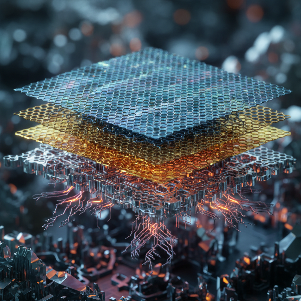
In the last few years, the field of photovoltaics has moved beyond single 2D flakes toward deliberately engineered van der Waals heterostructures — precisely stacked, atomically sharp interfaces of different two‑dimensional materials. These assemblies combine the unique excitonic physics of monolayers with designer band alignments and interlayer coupling, enabling rapid charge separation, new absorber spectra and device form factors such as flexible, semi‑transparent and ultra‑thin tandem cells.
How these heterostructures change the rules
Two features distinguish 2D heterostructure photovoltaics from conventional thin films:
- Interlayer excitons and ultrafast charge transfer. When two transition‑metal dichalcogenides (TMDs) such as WSe2 and MoSe2 are stacked, photoexcited electrons and holes can localize in neighbouring layers. Ultrafast spectroscopy studies show that charge transfer across these van der Waals interfaces can occur on femtosecond to picosecond timescales, reducing recombination and promoting directional current extraction.
- Tunable band alignment and absorption engineering. Layer choice, stack order and twist angle allow continuous tuning of type‑I, type‑II or broken‑gap alignments, and moiré superlattices can create novel sub‑bandgap states. That tunability supports selective absorption, hot‑carrier strategies and engineered cascade extraction for tandem configurations.
- Atomically sharp interfaces with low defect densities. Because 2D crystals lack dangling bonds, stacked interfaces minimize recombination centers when fabricated cleanly — a key advantage for exciton preservation and efficient charge transfer.
Why it matters now
Commercial silicon and thin‑film technologies will continue to dominate bulk power generation, but 2D heterostructures unlock application spaces that conventional cells struggle to address: ultra‑lightweight photovoltaics for aerospace, conformal skins for building‑integrated photovoltaics, and spectrally selective subcells for compact tandem devices. Moreover, the inherent tunability offers a scientific playground for testing concepts such as hot‑carrier extraction, intermediate bands and moiré‑mediated absorption — strategies that could eventually raise practical device efficiencies beyond current limits.
Remaining bottlenecks
Despite intense progress at the lab scale, several barriers constrain near‑term deployment:
- Low per‑layer absorption: A single monolayer absorbs only a few percent of incident light. Practical devices require light trapping, multi‑stack strategies or hybrid integration with thicker absorbers.
- Scalability and reproducibility: Mechanical exfoliation and small‑area transfer yield exceptional devices, but wafer‑scale growth with the same interface quality remains an industrial challenge.
- Contacts, stability and encapsulation: Making low‑resistance, long‑lived contacts without disrupting delicate interlayer physics is nontrivial, and many 2D materials are sensitive to oxygen and moisture.
Outlook
Research is converging on hybrid pathways: combining 2D heterostructures with established photovoltaic absorbers (silicon, perovskites) to realize efficient tandems or to provide functional layers that improve carrier extraction and spectral management. Continued advances in chemical vapour deposition, dry transfer and contact engineering — alongside fundamental work in exciton dynamics and moiré physics — will determine whether 2D heterostructures remain primarily a scientific platform or become a practical complement to conventional solar technologies. For now, they are both: a rich arena for discovery and an increasingly plausible route to application‑specific, next‑generation photovoltaics.